Mr. Samanyu Kumar and Mr.Krishna Aswani came from Banaras Hindu University by NIMS Internship Program from May 19.
2010.10.6
Dr. Anirban Bandyopadhyay's nano-brain research picture became one of the best 25 selected research work of
The Japan Foundation of Public Communication on Science and Technology
Royal Society of Chemistry interviewed with Dr.Anirban Bandyopadhyay regarding The many faces of a single molecule
The paper was selected for the Cover Page, please find it above, and to read the paper, please follow the link http://www.rsc.org/publishing/journals/CP/article.asp?doi=B913691F*"
"Our group member Dr. Anirban Bandyopadhyay has become World Technology Network (WTN) Fellow on 16th of July
at New York USA. The Fellow position has been awarded to the top five creative materials scientists in the world."
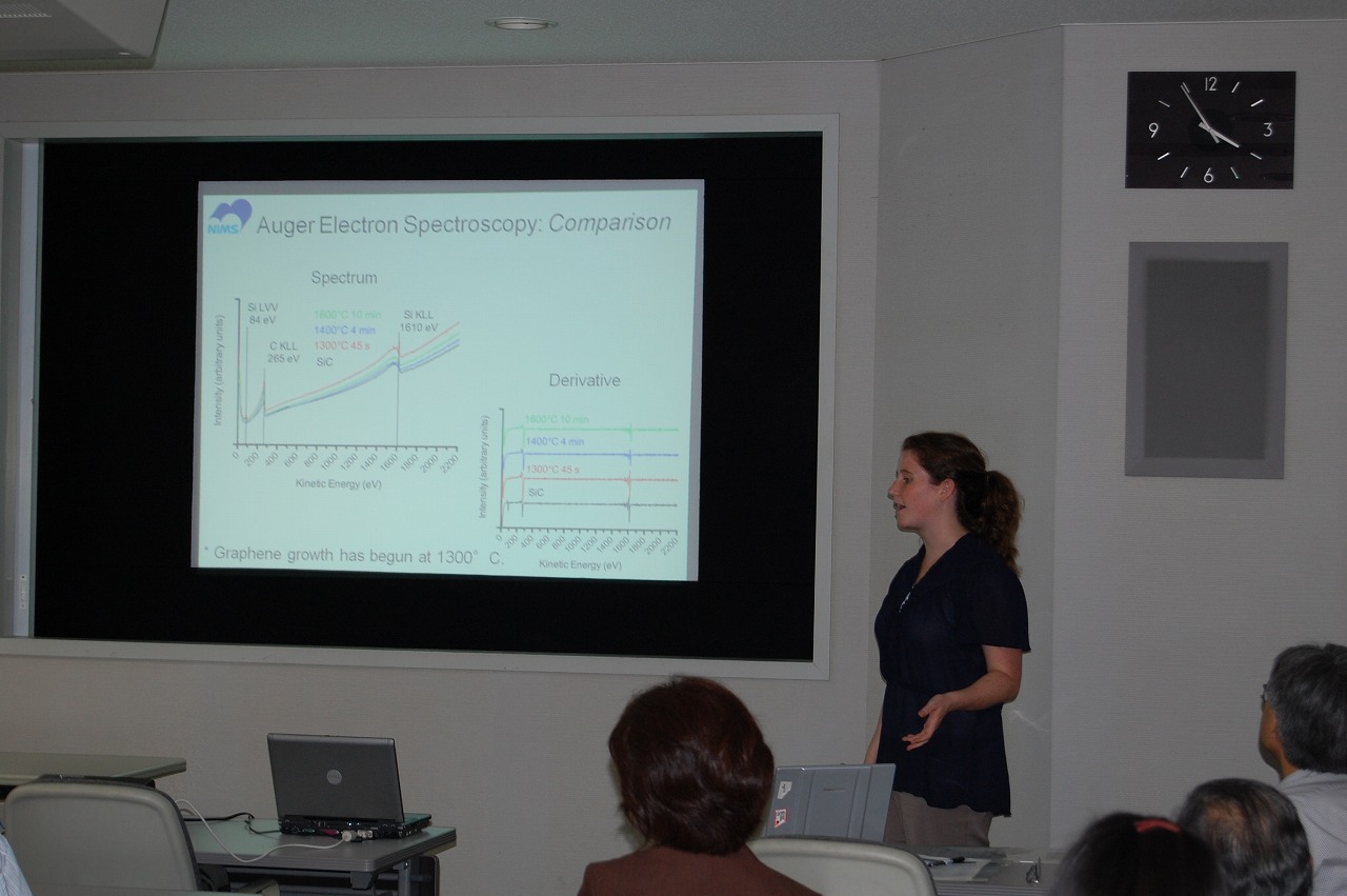 Research Presentation on Aug.6,2009
NNIN/NIMS Intrnship Students, Julie Stiver from University of Massachusetts, Amherst gave a talk.
Title ”Growth and Characterization of Graphene on Silicon Carbide”
 Mr. Jan Pudl joined our group from Dec.3, 2007 as an inturn from Czech
for a 1 year inturnship.
Mr. Jan Pudl joined our group from Dec.3, 2007 as an inturn from Czech
for a 1 year inturnship.  According to NIMS Internship Program 2007, Mr.Yuvra Pathak was invited
to our group.He presents the results of his study "Studied the electrical
properties of FULLERENE NANOTUBES USING A CONDUCTIVE AFM" July. 7,, 2007
According to NIMS Internship Program 2007, Mr.Yuvra Pathak was invited
to our group.He presents the results of his study "Studied the electrical
properties of FULLERENE NANOTUBES USING A CONDUCTIVE AFM" July. 7,, 2007Dr. Fujita and Dr.A.Itakura were appointed as an Adjunct Professor with the Faculty of Mathematics and Physics, Charles University in Prague.
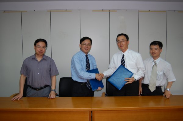 Sign MOU withNational Laboratory for Physical Sciences at the Microscale(HFNL),
University of Science and Technology of China(USTC)
Sign MOU withNational Laboratory for Physical Sciences at the Microscale(HFNL),
University of Science and Technology of China(USTC)June 7,2007
 Ms.Onishi received the award for contribution to exchange with local community
and NIMS on Apr. 1, 2007
Ms.Onishi received the award for contribution to exchange with local community
and NIMS on Apr. 1, 2007  Dr. D.Fujita is a member of the International Advisory Boards of The Special Symposium “Disclosing Materials at Nanoscale” of the 11th International
Ceramics Congress of CIMTEC 2006
Dr. D.Fujita is a member of the International Advisory Boards of The Special Symposium “Disclosing Materials at Nanoscale” of the 11th International
Ceramics Congress of CIMTEC 2006 Acireale, Sicily, Italy June4-9,2006
 Proceedings of APF9 was published in Applied Surface Science
Vol. 241 (2005)
 Following review article has been published in the latest issue of 「OYOBUTURI」
Vol.74, No.2, pp.208-212 Feb.2005,
Following review article has been published in the latest issue of 「OYOBUTURI」
Vol.74, No.2, pp.208-212 Feb.2005,"Manipulation of asymmetric dimer phases on Si(001) by using low-temperature scanning tunneling microscopy" by D.Fujita and K.Sagisaka